
Page 13 - Ten_HSD_Rules
P. 13
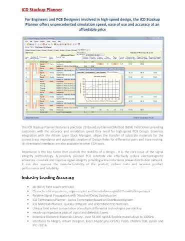
iCD Stackup Planner


                  For Engineers and PCB Designers involved in high-speed design, the iCD Stackup
                  Planner offers unprecedented simulation speed, ease of use and accuracy at an

                                                     affordable price


               The iCD Stackup Planner features a precision 2D Boundary Element Method (BEM) Field Solver providing
               customers  with  the  accuracy  and  simulation  speed  they  need  for  high-speed  PCB  Design.  Seamless
               integration  with  the  Altium  Layer  Stack  Manager,  allows  the  transfer  of  substrate  materials  for  the
               correct trace impedance and automatic creation of Design Rules for differential pairs and trace routing.
                Bi-directional interfaces are also available to other EDA tools.


               Impedance is the key factor that  controls  the stability of a design - it is the core issue of  the signal
               integrity  methodology.  A  properly  planned  PCB  substrate  can  effectively  reduce  electromagnetic
               emissions, crosstalk and improve signal integrity providing a low inductance power distribution network.
               It  can  also  improve  the  manufacturability  of  the  product;  reduce  costs  and  increase  product
               performance and reliability.


               Industry Leading Accuracy


                   •  2D (BEM) field solver precision
                   •  Characteristic impedance, edge-coupled and broadside-coupled differential impedance
                   •  Relative Signal Propagation with 'Matched Delay Optimization'
                   •  iCD Termination Planner - Series Termination based on Distributed System
                   •  iCD Materials Planner - quickly compare  and select dielectric materials
                   •  Unique field solver computation of multiple differential technologies per stackup
                   •  Heads-up impedance plots of signal and dielectric layers
                   •  Extensive Dielectric Materials Library - over 33,000 rigid & flexible materials up to 100GHz
                   •  Interfaces to Allegro, Altium Designer, Excel, HyperLynx, OrCAD, PADS, ZMetrix TDR, Zuken and
                       IPC-2581B